- Silicon carbide (SiC) semiconductors are key to making electric vehicles more efficient and increasing their range. Bosch is driving development forward by introducing its third generation SiC MOSFETs.
- Gen 3 SiC semiconductors build on Bosch’s proven dual-channel trench architecture, advancing it through four upgrades that improve performance, robustness, and heat dissipation.
- A 20 percent reduction in specific on-resistance, around 10 percent higher short-circuit withstand capability, and a 40 percent thinner die enable clear efficiency gains and more cost-effective power module designs.
- Gen 3 silicon carbide MOSFETs support the transition from premium EV applications to broader vehicle segments.
Evolution takes us to the future, one step at a time. In nature, it operates gradually, enabling a species to withstand greater stress, occupy new habitats, and flourish where others cannot. In power electronics, the logic is strikingly similar. With the introduction of Bosch’s third-generation SiC MOSFETs we are taking the next step in a gradual evolution, achieving greater performance and robustness in ever smaller chips.
Gen 3 SiC technology improves overall performance and optimizes the balance between efficiency and ruggedness – a key objective throughout Bosch’s power electronics evolution. At the same time, the reduced die size has a direct impact on production efficiency and system-level costs, further supported by the transition to 200 mm wafer manufacturing, which increases chip output per wafer. While Bosch’s SiC chips are already well-established in the demanding environment of high-performance electric vehicles, Gen 3 now aims to extend across the entire EV spectrum, from premium sports cars to mass-market models.
Ready to take the next evolutionary step
The starting point is Bosch’s proven vertical trench architecture. Its dual-channel design maximizes the active area for current conduction by using both sides of the gate trench. This increases channel density and decreases resistance, a key factor in how a MOSFET works in high-efficiency switching circuits. Deep p-type shielding regions protect the gate structure and limit saturation current in short-circuit scenarios. It is a mature design widely used in power semiconductor applications such as traction inverters. However, even proven semiconductor architectures offer room for refinement. This is where Gen 3 comes into play: as the next evolutionary step in SiC MOSFET technology.
The changes of Gen 3 in numbers
Gen 3 SiC MOSFETs offer measurable improvements in three key areas for automotive applications: electrical performance, thermal performance, and ruggedness.
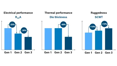
Electrical performance: Gen 3 delivers a 20 percent reduction in RonA compared to Gen 2. This reduces conduction losses and increases inverter efficiency, enabling smaller chip areas and more compact, cost-efficient designs. Improved capacitance characteristics contribute to a reduction in switching losses of around 10 percent during typical traction inverter operation.
Thermal performance: Reducing die thickness by 40 percent directly enhances heat dissipation and thermal conductivity. This supports higher power density and more efficient thermal management in high-performance semiconductor systems.
Ruggedness: The short-circuit withstand capability increases by about 10 percent, supported by the optimized two-zone JFET region and enhanced gate oxide design. The design also improves robustness against parasitic turn-on at high switching speeds. Additionally, the intrinsic body diode is optimized for soft recovery behavior across the full automotive temperature range of -40°C to 200°C, reducing electrical stress during switching events and supporting stable operation under demanding conditions.
Four architectural upgrades
These performance and robustness improvements stem from four architectural modifications in Gen 3, which maintain the strengths of the Gen 2 architecture.
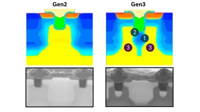
Firstly, an additional p-type shielding region was introduced directly below the trench, which provides full protection against off-state electric fields. This contributes to improved long-term gate oxide reliability under typical operating conditions. The existing hard mask of the trench etching process was reused for the new trench shield implant, eliminating the need for an additional lithographic process step.
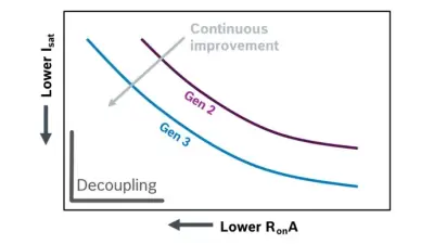
Secondly, Gen 3 features a two-zone structure in the JFET region beneath the trench, a geometrical current constriction between adjacent p-body regions that defines the current path and strongly influences both current density and electric field distribution. Each channel now corresponds to its own JFET region, providing significantly finer control over electric field distribution during both normal operation and fault events. This substantially improves the critical trade-off between on-resistance (RonA) and short-circuit withstand time (SCWT), expanding the available design space for robust, high-performance SiC power semiconductors.
Lastly, the die thickness in Gen 3 is reduced by 40 percent to only 100 µm. This reduces material usage and places the active semiconductor layer closer to the heat sink, accelerating heat dissipation.
Sign up for full access
Sign up freeAlready an account ? Log in

Global Semiconductor Trends
Semiconductors in the AI era: more value, not more silicon

Computing and Software
AI, auto, and advanced packaging: the semiconductor industry’s next data-driven era

Sensing and Actuating
Sensing, imaging, and RF: the three pillar technologies serving “physical AI”

Compound Semiconductor
EigenQ Secures $45 Million Financing Ahead of Planned Listing

Compound Semiconductor
IBM’s Anderon lands $1B CHIPS award for US quantum wafer foundry

Memory
Infineon enters into agreement to sell NOR Flash and F-RAM business to Winbond and sharpens focus on core growth areas

Imaging
STMicroelectronics introduces automotive image sensor to help scale affordable in-cabin sensing

Compound Semiconductor
Sparrow Quantum Sets Record With 500 Million Usable Photons Per Second

Compound Semiconductor
NEC Halts Development of Quantum Computer Hardware

Compound Semiconductor